Introduction: The Importance of Implant Quality Control
Ion implantation is a cornerstone process in semiconductor manufacturing. It introduces dopant atoms into silicon and other substrates. Traditionally this has been done to modify electrical properties, forming the p-n junctions and channel regions that transistors and other devices rely on. Additional use cases for advanced node manufacturing are also emerging, using implant to modify other material properties, for instance to assist in the etch process. Because device behavior (like transistor threshold voltages and leakage) is extremely sensitive to dopant concentrations and depths, characterizing implant profiles is critical. Even small deviations in implant dose or depth can lead to non-uniform device performance and yield loss. In high-volume fabs and equipment manufacturing, robust implant characterization underpins quality control, and is vital for consistent, reliable semiconductor device fabrication.
Modern fabs treat implant characterization as part of their overall process control strategy, not just a one-off R&D measurement. For example, Secondary Ion Mass Spectrometry (SIMS) depth profiling is often used to qualify ion implanter tools and monitor processes, sometimes even serving as a gating metric for process changes. By detecting chemical impurities and dopant levels down to trace levels, SIMS helps catch issues that other in-fab monitors might miss, which can save costly troubleshooting later. Good implant characterization helps identify problems early -- whether it's a drifting implanter, a contamination issue, or an incorrect process recipe -- before they wreak havoc on product wafers.
Dopants and Device Performance: Depth, Dose, and Isotopes
In semiconductor devices, key transistor parameters are directly tied to how many dopant atoms are in a region (dose), how deeply they penetrate (profile shape and depth), and how they are activated (often via annealing). For instance, a MOSFET's channel doping sets its threshold voltage, and source/drain implants create the junction depths that control short-channel effects and leakage. If an implant dose is too low, devices might not turn on as expected; too high, and junctions might overlap or parasitic capacitances increase.
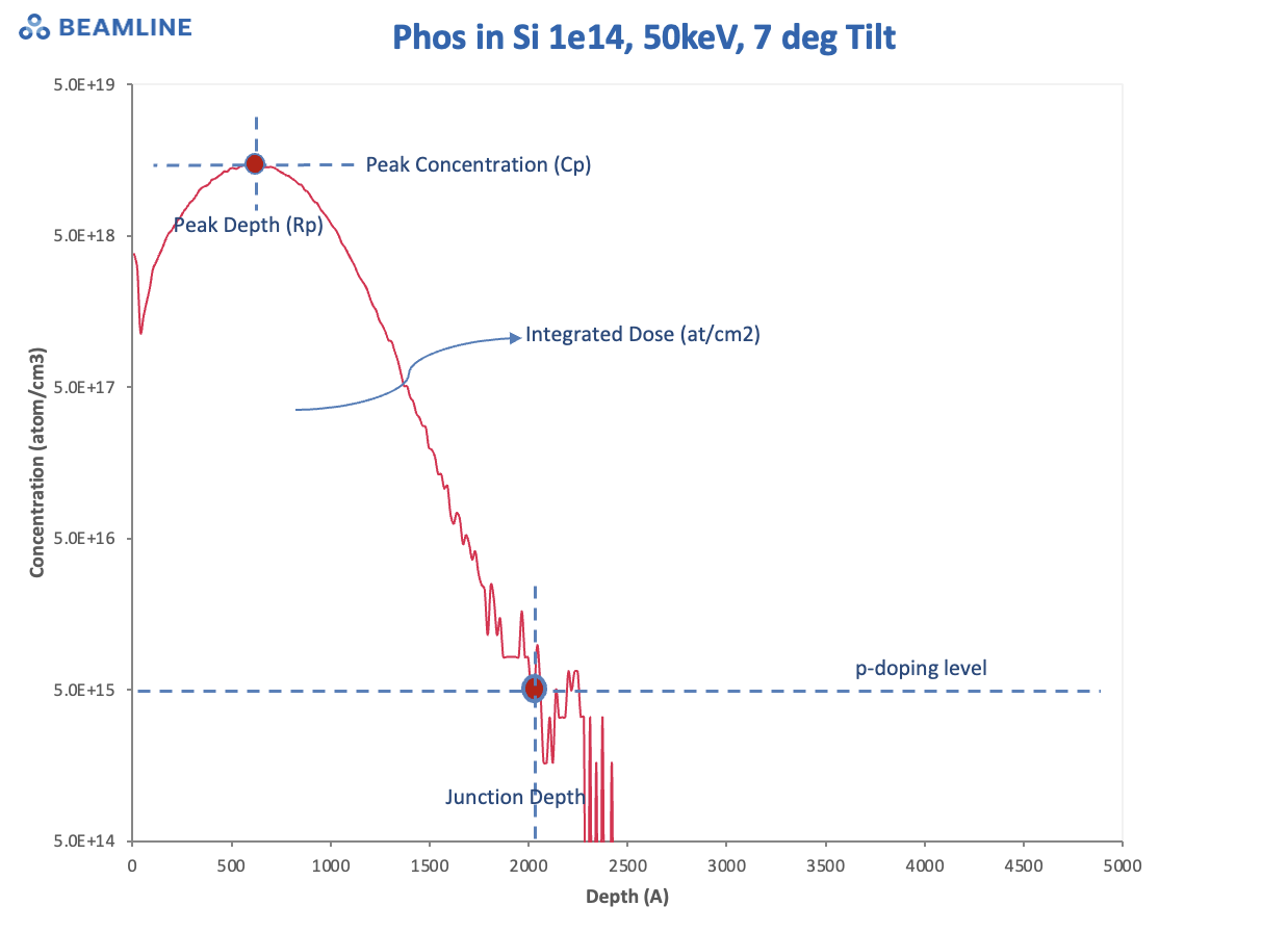
Likewise, if the dopant is too deep or too shallow, the transistor's on/off characteristics and speed can deviate from design targets. Implant profiles typically follow a somewhat Gaussian distribution in depth, with a peak concentration at a certain depth determined by implant energy and a tail that falls off deeper in the silicon. The tail portion can be critical -- an excessively long tail (dopant atoms drifting too deep) can cause unexpected sub-surface leakage paths or punch-through in devices, whereas a very abrupt profile might lead to abrupt junctions that increase series resistance.
Not only the concentration and depth matter, but which dopant species is used can have different effects. Common dopants like boron (B), phosphorus (P), and arsenic (As) each have different atomic masses and diffusivities, resulting in different as-implanted profiles and diffusion behaviors. Heavier ions like As tend to create shallower profiles for a given energy (due to more scattering), whereas lighter ions like B penetrate further at the same energy. Additionally, some dopants are introduced as molecules or complexes (for example, BF₂ for boron implants), which can affect the implant profile shape and lead to co-implanted species (like fluorine in the case of BF₂). These nuances mean that process engineers must choose dopant species carefully and often rely on empirical characterization to see the actual distribution. In some cases, even dopant isotopes come into play. While isotopes of an element (like 10B vs 11B) behave virtually identical electrically, they can be leveraged in experiments -- for example, using an enriched isotope implant as a tracer. Distinguishing isotopes of the same element by mass can be incredibly useful for diagnosing issues like cross-contamination (e.g. detecting a bit of 11B in what should be a 10B implant) or studying diffusion by marking one source with a rare isotope.
Ultimately, getting the dopant dose and depth right is essential to meeting device performance targets. As device geometries have shrunk and new materials are introduced, the tolerances on implants have tightened -- there is far less margin for error today. This is why implant characterization is so important: it provides the data needed to verify that dopant atoms are indeed where they're supposed to be. If the dopants define the device, then measuring those dopants can define the difference between success and failure in production.
Key Variables in Ion Implantation (and Why They Matter)
Ion implantation might seem straightforward -- set the desired dose and energy and fire away -- but in practice it's a complex process with many variables. Each of these variables can alter the resulting dopant profile. Here are some of the key parameters and how they affect implants:
During implantation, wafers are typically tilted a few degrees off the ion beam axis and sometimes rotated (twist) to avoid channeling. Channeling is a phenomenon where ions travel long distances along crystallographic channels, leading to much deeper penetration than intended. If the tilt angle is set incorrectly or the beam alignment is off, dopants can channel, resulting in profiles that are deeper than expected (or exhibit strange dual-peaks). Most production implants deliberately use a small tilt (like 7°) because on-axis implants would be extremely sensitive to tiny alignment errors. A problem in the tilt/twist calibration of the implanter can therefore cause significant variations. Engineers monitor this because angle errors often show up as shifts in profile depth or abnormal dopant tails. In short, implant angle control is critical to achieving the desired depth distribution and avoiding unintended channeling.
The ion beam acceleration energy sets how deep dopants go -- higher energy implants penetrate further (higher range). A low-energy implant might place peak dopant concentration only a few tens of nanometers deep, whereas a high-energy implant can reach microns into the wafer. However, energy purity is an often overlooked aspect: ion implanters produce a beam of mostly the desired energy, but there can be traces of higher or lower energy ions (for instance, doubly charged ions that come through the mass separator, or molecular clusters). These out-of-spec energy components lead to tails in the implant profile (e.g., a small fraction of dopant ions going much deeper than the main population. This is especially important in sensitive applications -- for example, in shallow junction formation, a high-energy tail could punch through the junction, or in materials modification implants (non-electrical implants used to tweak material properties), unwanted depth distribution can undermine the intended modification. Thus, controlling and characterizing the energy distribution of the implant is vital. If a profile's tail is longer than expected, it might indicate energy contamination or beam filtration issues in the implanter. In the case of technology transfer in mature processes, new tools often have better energy contamination control, and therefore the opposite can be true: if the profile's tail is shorter than expected the process may have to be modified (such as adding additional implants) to match the characteristics of legacy tooling.
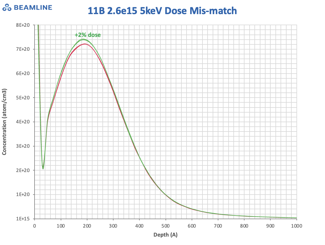
This is the amount of dopant per area. It directly affects the peak concentration of dopants in the profile (higher dose → higher peak, assuming the same area distribution). Dose accuracy is a fundamental concern -- implant tools have dosimetry systems (faraday cups measuring beam current) to regulate dose, but errors can occur. Calibration drift, beam current measurement errors, or charge neutralization issues can cause actual dose to deviate from the setpoint. For example, if the beam current is partially neutralized by a poor vacuum (excess gas leads to charge exchange), the dose monitor might under-count ions. The tool could then overdose to compensate, resulting in higher actual dose. Such subtle issues mean that a dose verification by an independent method is often done on test wafers. Process engineers must consider that the dose delivered can be influenced by tool maintenance, source life, or even things like wafer charging (hence the use of plasma flood guns to neutralize charge on insulating wafers). Achieving the correct dose, and a uniform dose across the wafer, is paramount for uniform device behavior.
Implants behave differently depending on the substrate. In single-crystal silicon, dopants can channel along crystal planes if the beam goes in at certain angles. In contrast, an amorphous or polycrystalline target (or a different semiconductor like GaAs or SiC) will scatter ions more randomly. For example, high-mobility materials (Ge, III-V semiconductors, etc.) are increasingly being used in advanced devices, widening the range of elements and implant conditions used. Each new material can introduce different range profiles and damage behaviors, so understanding substrate effects is crucial. Even the substrate's initial dopant concentration (background doping) can matter, as it might slightly alter stopping power or lead to self-compensation effects that counteract the effect of the dopant.
After implantation, dopants typically need to be electrically activated and any implant damage (amorphization) needs to be repaired. This is done by annealing (thermal budgets can range from rapid spike anneals to longer furnace anneals). Annealing can also cause dopants to diffuse from their as-implanted locations. For example, boron can diffuse rapidly at high temperatures, which can broaden the profile and shift the junction depth. In process development, it's important to know if an observed profile issue is from the implant itself or from the subsequent anneal. Characterizing an as-implanted profile versus after anneal can isolate the effect of the annealing step. Key variables like anneal temperature and time will interact with the implant profile -- a too-aggressive anneal could "smear" out a shallow implant, while an insufficient anneal might leave damage or unactivated dopants. Process engineers thus treat anneal and implant as a coupled pair of steps when tuning device performance. In some advanced processes, alternative curing methods (like laser anneal or flash lamps) are used to limit diffusion while activating dopants.
Typically, implants are done at room temperature, but there are special cases where cryo implants or heated implants are used. Cryogenic implantation (cooling the wafer, sometimes to liquid nitrogen temperatures) can suppress dynamic annealing effects, leading to higher damage (amorphization) which can be beneficial for certain dopants in SiC or to prevent transient diffusion on anneal. Hot implants (e.g., implanting SiC at 500 °C) can help reduce damage for materials that are otherwise hard to anneal. Both cases add complexity: a cryo stage or a heated stage must uniformly control wafer temperature. If the stage cooling/heating is uneven, different parts of the wafer might get different implant profiles (due to differing damage states). This is a known challenge: controlling the wafer temperature uniformly is outside the core beam physics that implanter manufacturers specialize in, and historically, some heated implant stages had uniformity issues across the wafer. Cryogenic implants are similarly tricky -- if one wafer is a few degrees warmer than another, the end-of-range damage and dopant diffusion upon anneal might differ. The takeaway is that when using non-room-temperature implants, engineers must carefully characterize profiles across the wafer and from wafer to wafer to ensure consistency. Multiple measurement points (center vs edge) might be needed to confirm within-wafer uniformity. Any observed non-uniformity in device performance across a wafer could hint at temperature control issues during implant.
All these variables -- and others like beam current density, implant mask pattern effects (shadowing from photoresist topography), and more -- interplay to determine the final dopant distribution. Because there are so many knobs, implant engineers rely on characterization data to verify and fine-tune each one. For example, when transferring a process to a new tool or a different fab, they might run a set of witness wafers through a "matrix" of angles, energies, doses, etc., and then use metrology to compare the outcomes. Only by measuring the actual profiles can they confidently match the process to the previous baseline. As the saying goes: "If you don't measure it, you can't control it." And nowhere is that more true than with ion implantation.
Common Implant Issues and Their Root Causes
Despite best efforts, things can and do go wrong with ion implants -- both in day-to-day production and during new process development. Here we'll highlight some common implant issues that engineers encounter, and what often causes them:
If devices are coming out consistently fast or slow, or parametric tests show implausibly low/high dopant activation, the implant dose could be off. Under-dosing means not enough dopant was implanted; over-dosing means too much. Root causes can include mechanical issues, mis-calibration of the implanter's dosimetry system, drift in the ion source beam current, or issues like beam neutralization.
Here the overall shape of the dopant profile is shifted -- maybe the peak is nanometers shallower than it should be, or the junction depth is deeper. A too shallow profile could result in insufficient junction depth, potentially causing high resistance or threshold shifts; too deep could cause punch-through or leakage issues. Common causes include errors in implant energy setting or beam energy contamination.
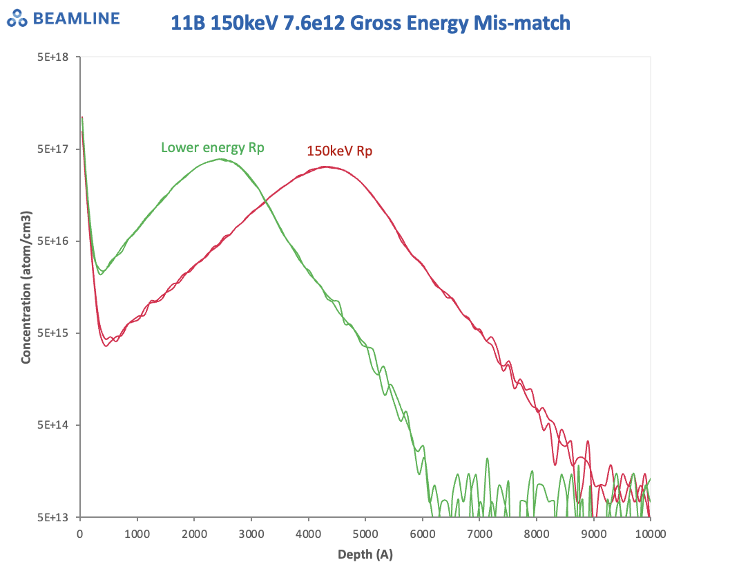
For instance, if the ion source produces an unexpected fraction of doubly-charged ions, they will implant at roughly twice the intended energy, creating a deeper secondary peak or tail. Another cause can be wafer misorientation -- if a wafer was accidentally implanted on-axis (0° tilt) when it should have been tilted, heavy channeling could drive dopants deeper than intended. A depth profile is often the fastest way to diagnose this: it will clearly show if the distribution is shifted or oddly shaped compared to the expected profile simulation. Once identified, engineers might check the implanter's energy calibration or inspect if the wrong beamline recipe was used (for example, using the wrong mass filter settings letting unwanted species through). In modern tools, energy purity (to minimize those tails) is a big focus -- so if profiles start showing abnormal tails, it might even indicate a maintenance issue like a degraded mass analyzer magnet or a failing vacuum component that is allowing molecular fragments into the beam.
As discussed earlier, channeling can cause deeper penetration. One manifestation is strange twin-peaks or shoulders in the dopant profile -- one peak from the channeled portion and one from the normal distribution. If devices on one side of a wafer are different from the other, one possibility is that the implant angle was a bit off (say the wafer wasn't perfectly flat or the platen tilted slightly), so part of the wafer got a more aligned beam (more channeling). The root cause could be a misalignment in the tool hardware or an incorrect setup in the recipe. Tilt/twist angle errors often show up during routine tool qualifications: fabs will do a set of implants at slightly different angles and measure them to ensure the tool is implanting as expected. Should a channeling issue be found, recalibrating the tilt or fixing the mechanical alignment usually resolves it. Channeling can also occur if the substrate crystallography is different (e.g., implanting into a wafer that has a different crystal orientation than usual), so that's checked as well.
Ion implanters are used for many species, and sometimes the previously implanted species can contaminate the next implant. An example is phosphorus memory effect: after a high-dose P implant, some phosphorus can stick around in the chamber, and if the next job is a boron implant, you might inadvertently implant a bit of phosphorus along with the boron. This becomes an "anti-dopant" contamination -- phosphorus (donor) counter-doping regions that were supposed to be p-type, for instance. The result can be devastating for devices: the two dopants compensate each other, yielding lower active doping than intended, or creating unwanted junctions. Metals from components can also sputter off and get implanted (e.g. tungsten from ion source filaments, or steel from chamber walls. Preventative maintenance and proper source cleaning/beamline tuning are key to minimizing cross-contamination. Good data data can flag unexpected species in a profile, and help reduce the uncertainty of the troubleshooting process.
Sometimes an implant issue isn't about the dopant at all, but extraneous contamination. While contaminants are usually not successfully implanted, if a wafer shows an odd localized dopant spike or devices fail in a cluster, a particle might be to blame. Large particulates in the beamline can shadow areas or sputter material into the wafer, causing strange readings. For example, a flake from the ion source might suddenly come off and either block implants (causing a "shadow" -- no dopant in one spot) or itself implant as a micro-contaminant (e.g., a fleck of nickel that then implants Ni ions where it lands). These particle events during materials modification curing implants can also introduce a "false mask" on the resist leading to erroneous downstream etch patterning. End-station contamination like backstreaming pump oil or a sudden outgassing can also introduce elements onto the wafer during implant. These incidents are often stochastic, but metrology can later analyze the affected wafer and identify any unusual elements present, which helps root-cause the contamination (e.g., finding a bit of fluorine and carbon might point to a vacuum grease contaminant). Routine monitoring of common contaminants (O, C, F, metals) by sensitive techniques helps ensure the implant tool and environment are clean.
Ideally, every point on the wafer gets the same dose and profile. But sometimes within-wafer non-uniformity creeps in -- for example, the center of the wafer gets a slightly lower dose than the edges, or vice versa. Engineers colloquially refer to certain patterns like a "donut" profile (higher dose at edge, lower in center) versus center-heavy, etc.
Causes can range from beam scanning issues (if the ion beam doesn't sweep evenly, perhaps due to a glitch in scanner magnets) to platen tilt or temperature non-uniformity (as mentioned, for cryo implants, the center might cool differently than the edge). Another cause is shadowing by tooling -- on some implanters, parts of the machine (like mechanical fixtures) can partially block the beam at extreme angles or edges if not perfectly adjusted. When non-uniform implants occur, device parametrics across the wafer will vary systematically. The root cause investigation often uses multiple depth measurements across the wafer radius to map out the actual dopant distribution in different regions. If a pattern emerges (say, gradually dropping dose toward one side), it can implicate a mechanical issue (maybe the beam isn't centered properly or the wafer clamping is off-level). While implanter vendors often provide specifications for within-wafer uniformity, it's important to verify those specs and monitor uniformity long term.
Beyond the pure dopant profile, implants cause lattice damage, and sometimes issues arise from that damage. High-dose implants amorphize the silicon surface; if not managed, this can cause device variations or additional diffusion upon anneal. Amorphization issues might manifest as differences in how well the dopant activates or how the subsequent anneal behaves (e.g., end-of-range defects causing leakage). One interesting example: implants can impact etch rates in subsequent fab steps. If one wafer received a heavier implant in a certain region, that region's silicon crystal is more damaged and will etch faster in an etch process (since etch chemistry attacks disordered silicon more readily). This can lead to features etching differently than intended -- an effect sometimes seen in patterning levels where an implant is done through a hard mask. Engineers have found that differences in implant conditions can explain unexpected etch bias or etch rate differences across a wafer. The root cause is the implant damage altering material properties (e.g., making photoresist or oxide more porous to etchants, or silicon more susceptible to etch). Solutions include adjusting the implant recipe (like beam current, beam density, dose, or temperature) to minimize unwanted damage or compensating in the etch recipe.
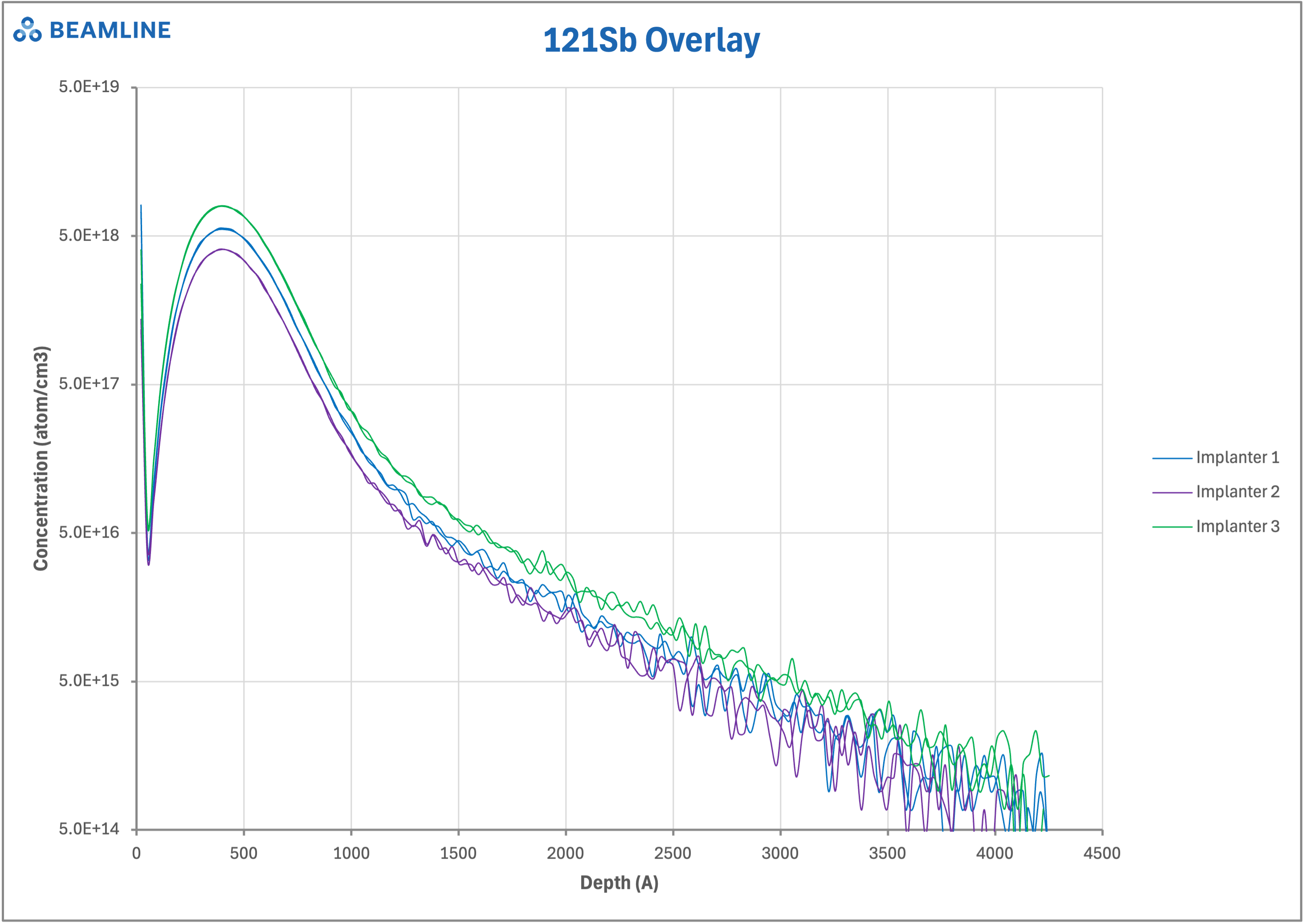
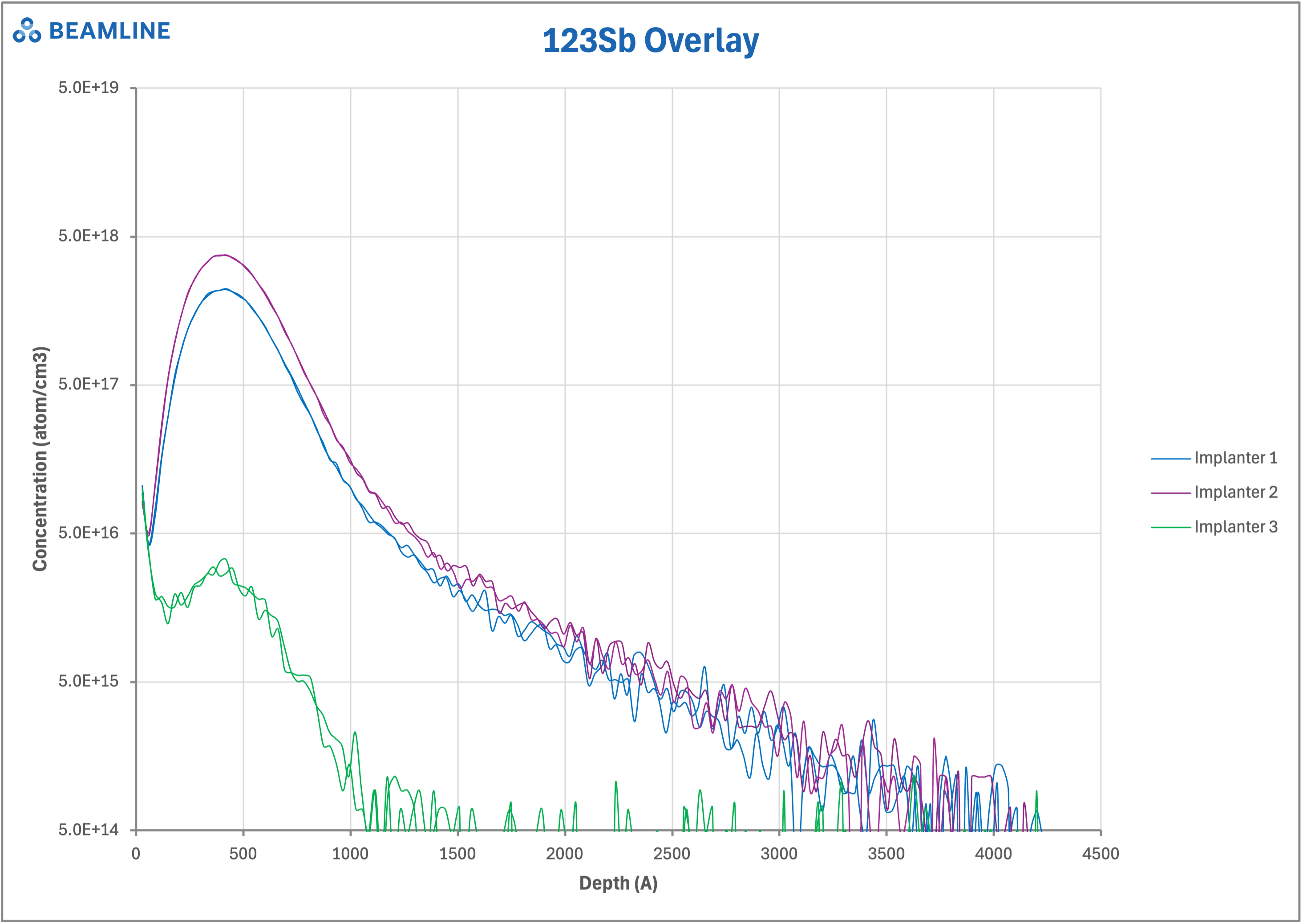
It's worth noting that many implant issues correlate with changes in the fab -- such as a new implanter coming online, a recent preventative maintenance (PM) on the tool, a new batch of dopant source gas, or a process transfer from one fab to another. Engineers know to be extra vigilant with characterization during these times. For instance, after PM event, they may run a few calibration wafers to check that profiles and doses still match the previous baseline. Or when transferring a process, doing a overlay depth profile comparison between the old tool and the new one ensures that things like angle alignment and energy match are spot on. If issues are found, it could be due to subtle differences in hardware that need fine-tuning. Thus, implant characterization isn't only for when things go wrong -- it's a preventative tool to keep the implant process running smoothly through changes. Understanding and controlling variability in performance between PMs, ensuring predictable equipment operation between PMs, and minimizing tool downtime (e.g. "green-to-green time") are all ways that good characterization directly provides value and impacts the bottom line of a fab.
In all these scenarios, measuring the actual dopant depth profiles, concentrations, and any impurities, can provide the definitive evidence of what went wrong (or right). However, often these issues remain invisible to standard in-line monitors, because they lack the sensitivity required. Worse, end-of-line testing can happen weeks after the implant (as the device has to be built for such testing) and therefore potentially mean weeks worth of manufactured product that has to be scrapped. Good metrology turns what could be a very difficult troubleshooting puzzle into a more straightforward comparison against expected profiles, and reduces the time-based risk surface for excursions, reducing their frequency and cost. For example, seeing an unexpected phosphorus bump in a boron profile immediately fingers cross-contamination; noticing a deeper junction hints at channeling or energy problems; a uniform dose shift suggests dosimetry calibration error, and so on. Armed with this information, process engineers can then take corrective actions -- whether it's tweaking tool settings, performing maintenance, or adjusting the process flow -- to solve the implant issue.
Key Takeaways
- Essential for Implants: SIMS is crucial for characterizing ion implant profiles, ensuring dose and depth accuracy.
- Superior Metrics: Offers ultra-high sensitivity, wide dynamic range, and excellent depth resolution.
- Comprehensive Analysis: Provides full elemental and isotopic information, vital for troubleshooting.
- Beamline Expertise: Beamline SIMS delivers best-in-class precision, stability, and semiconductor-focused expertise.
- Prevents Yield Loss: Effective characterization helps identify issues early, preventing costly manufacturing problems.
Measuring Implant Profiles: Approaches and Why SIMS Stands Out
So how can we actually measure the dopant distribution and verify those implant conditions to a high degree of certainty? In many production environments, a quick way to monitor implants is by measuring the sheet resistance (Rs) of a wafer after implant and anneal. Four-point probe tools can give a sheet resistance which correlates to dopant activation and dose. This is great for routine monitoring because it's fast and non-destructive for test wafers. If the Rs is too high or too low, it flags a dose issue or activation problem. However, sheet resistance is an indirect measurement -- it doesn't provide the actual dopant profile, just an aggregate effect of the dopant in an active layer. Different dopant depth distributions can yield the same sheet resistance, so it won't tell you if the profile shape is wrong. Also, Rs measurements lose sensitivity at very low doses or in very shallow implants (where the contribution to conduction is minimal or not measured). Hall effect measurements can separately give mobility and carrier density, but similarly they average over the depth. Spreading resistance profiling (SRP) is another electrical technique, where the wafer is beveled and the resistance is measured progressively, providing a depth profile of electrically active dopants. SRP can give good information for certain ranges but requires careful sample prep and isn't sensitive to inactive or low-level dopants. Overall, these and other electrical methods are invaluable for process control (especially for checking implant repeatability day-to-day), but they cannot fully characterize the profile shape or detect unintended impurities.
In additional, there are two major caveats for electrical testing:
First, while generally electrical measurements are considered non-destructive, the probe used for measurement DOES create localized damage. While often the measurement is taken on specifically manufactured "pads" to preserve the rest of the wafer, the same measurement cannot be taken twice, and therefore accuracy via repeatability testing is difficult.
And, second, as electrical tests can only be performed on activated dopants, the test is often performed post-anneal, and therefore any metrology reflects not just the activated dopant but also the healing of lattice damage, both of which are known to affect resistivity. Therefore, it is difficult to deconstruct the effects of the two processes, and truly monitor the implant step alone, just through this type of testing.
Given the limitations of electrical testing and other compositional analysis methods (which we will compare in a future article), Secondary Ion Mass Spectrometry (SIMS) has emerged as the go-to workhorse for implant characterization. Why? Because SIMS can do what other techniques can't: measure the full dopant depth distribution and detect tiny concentrations of impurities, all with high depth resolution. In a SIMS analysis, a small spot on the wafer is bombarded by a focused ion beam (like O₂⁺ or Cs⁺) which sputters the material; a fraction of ejected atoms (as ions) are collected and mass analyzed. By sputtering layer by layer, SIMS directly produces an elemental concentration vs depth profile. Here are the key reasons SIMS stands out for implants:
SIMS is one of the most sensitive analytical techniques available for solids. It can detect dopant and impurity levels down to parts-per-million, billion, or even trillion in some cases (Evaluating SIMS Vendors | Beamline). For context, 1 ppb in silicon is on the order of 10^13 atoms/cm^3. Many implants have peak concentrations around 10^18--10^20 atoms/cm^3 and tails that might drop below 10^15 atoms/cm^3 -- levels only SIMS can reliably measure in a profile. This ultra-low detection limit means SIMS can catch subtle contamination (like a 0.001% of unwanted species) and precisely measure low-dose implants or the faint dopant tail in a junction. Techniques like XPS would hit a wall at 0.1% (~10^18 atoms/cm^3), missing critical information. SIMS, on the other hand, has been demonstrated to detect key impurities in silicon at the parts-per-trillion level, which is why it's often used for contamination checks and equipment qualification in fabs.
Not only can SIMS see very low concentrations, it can measure a huge range of concentrations in one go. A single SIMS depth profile might start at a dopant peak of ~1e20 atoms/cm^3 near the surface and go down to 1e14 or lower in the tail -- that's 6+ orders of magnitude difference, all resolved continuously. In fact, modern SIMS can achieve up to 7 orders of magnitude dynamic range in concentration. This is essential for implant work, because you want to see both the peak and the tail of the profile clearly. Other methods often either saturate at the high end or fade into noise at the low end. SIMS's dynamic range ensures that the entire implant profile -- from the tops of the peaks to the deepest traces -- is captured. This is how SIMS simultaneously provides the dose (area under the curve), the peak concentration, and the junction depth info in one measurement, which is incredibly valuable for process characterization.
With careful tuning, SIMS can achieve excellent depth resolution, on the order of a few nanometers in the near-surface region for ultra-shallow implants, and it can profile depths from the very top atomic layers down to tens of microns into the bulk. The sputtering process is inherently a depth-grinding technique. By controlling the sputter rate and using appropriate primary ions (for example, O₂⁺ for electropositive elements, Cs⁺ for electronegative elements to enhance ion yield), one can optimize the depth profiling. For implant metrology, depth resolution matters because you want to know if your 20 nm junction is actually 20 nm or has blurred to 30 nm. SIMS profiles can resolve sharp dopant transitions -- and if the SIMS is convolving the profile slightly due to sputter-induced mixing, that can be deconvolved or minimized with optimized conditions. The ability to get depth information at high resolution is a key differentiator for SIMS versus any purely electrical measurement.
SIMS can detect essentially every element in the periodic table (H through U and beyond). Each element has a unique mass signature (often multiple, if you count isotopes), and SIMS will pick up whatever is present. This means in one depth profile, you might measure the dopant of interest and any other impurities that show up. For example, a single SIMS analysis could concurrently measure boron concentration and also check if there's any fluorine (from BF₂) or oxygen (contamination) as a function of depth. This all-elements capability is something electrical tests cannot do at all -- they only respond to electrically active dopants. Moreover, SIMS's ability to distinguish isotopes is a powerful advantage. As mentioned, one can intentionally use an isotope as a tracer or measure the ratio of isotopes to identify source contamination. For instance, chlorine has two major isotopes Cl-35 and Cl-37; if a process used a certain isotope enriched gas, SIMS could verify its incorporation specifically. In implant terms, the classic example is differentiating boron-10 vs boron-11. Natural boron is ~20% ^10B and 80% ^11B -- SIMS can not only measure "boron" but actually show the two isotope profiles. This might be used to confirm that an observed boron profile is indeed from a certain BF₃ source (which might have a known isotope ratio) versus background boron from chamber memory (which could potentially have a different ratio or be detectable in a previous SIMS scan on a clean wafer). No other technique gives this kind of nuanced insight.
SIMS is fundamentally a relative measurement (counts of secondary ions), but with proper calibration using standards, it provides quantitative concentration profiles. There are well-established implant reference materials (often NIST traceable) that labs use to calibrate their SIMS instruments for common dopants like B, P, As in Si. By measuring a standard sample with a known dose, the SIMS instrument's sensitivity factor can be determined, and then unknown samples can be quantified accurately. With good practices, SIMS quantification for implants can be on the order of < .7% RSD short term accuracy and ±5% sustained long-term precision for dose, which is usually more than sufficient for process control. The ability to get actual numbers (atoms/cm^3 versus depth) makes SIMS data directly comparable to device simulations and specifications. Engineers can take a SIMS profile and overlay it on TCAD simulation results or implant model predictions, enabling model validation and refinements. Competing methods like RBS are also quantitative but lack the sensitivity; electrical methods are quantitative to electrical activation but not total chemical concentration. SIMS nicely fills that role of quantitative chemical depth profiling.
SIMS can be focused to analyze a small area (on the order of tens of micrometers). This is useful if you need to profile a specific region of a wafer (say a test structure or a particular die). While implants are usually uniform, in some cases you want to check a particular feature -- SIMS can be combined with micro-patterning techniques (like small pads opened in oxide) to measure specific device regions without averaging across the whole wafer. This local analysis capability also means that SIMS can be used on product wafers (if you dedicate a scribe line location or use a test wafer that saw actual device patterning) to see effects of pattern density on implant, etc. Other techniques like sheet resistance average the whole wafer or a large region, possibly hiding such local effects.
Given all these advantages, it's clear why SIMS is the characterization method of choice for ion implantation. It's the only technique that simultaneously gives you the depth profile, the sensitivity, and the multi-element insight needed to truly understand an implant's outcome. This isn't to say SIMS is perfect -- it is a destructive analysis (it sputters a tiny crater in the sample) and it's typically an off-line measurement (conducted in a specialized lab, not on the production tool). But those are small trade-offs considering the wealth of information it provides. In practice, many fabs will do in-line monitors (like sheet resistance) on every lot for quick feedback, but then rely on periodic SIMS measurements for a deeper dive into the implant characteristics. For example, a fab might send one wafer a week to an external SIMS lab to ensure nothing has drifted in their process, or run a SIMS whenever a tool is refurbished or a new recipe is developed. The combination of fast in-fab electrical tests and detailed SIMS profiles is a common best practice.
Beyond implants, SIMS is also used to measure things like diffusion profiles, contamination in films, and stoichiometry of complex layers. But in the context of doping, it's truly the eyes of the process engineer inside the silicon (or other substrate)-- a way to see the invisible distribution of atoms that electrical tests only infer. When an implant issue arises, SIMS is usually the referee that settles what actually happened.
Beamline SIMS: Best-in-Class for Implant Characterization
Now that we've established why SIMS is uniquely suited for ion implant characterization, it's worth discussing why Beamline's SIMS Lab offers the best performance for this application. Beamline, a specialized SIMS service provider focused on the semiconductor industry, helps you achieve maximum precision, stability, and repeatability for measuring implant profiles.
What makes Beamline SIMS best-in-class? Let's break down the factors:
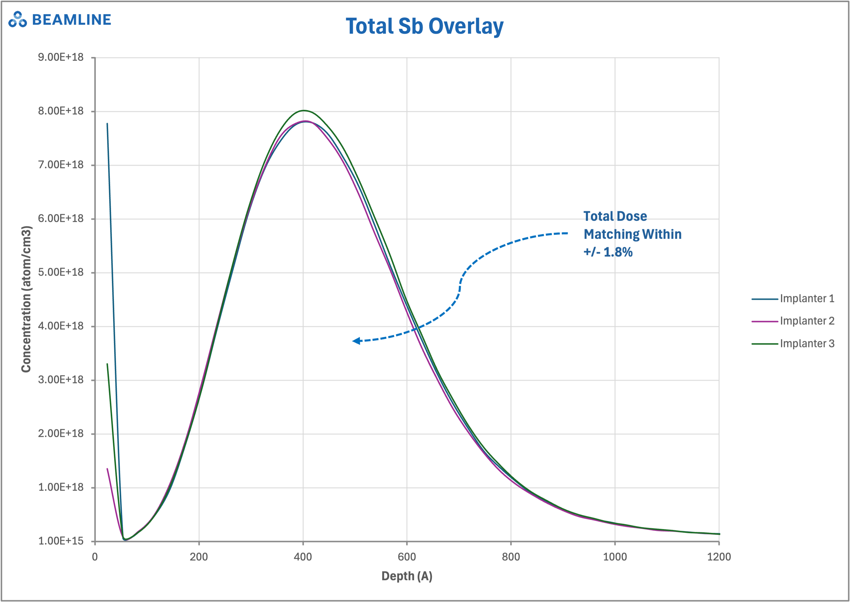
Beamline SIMS excels by rigorously tracking calibration standards and using stable conditions to ensure that a dopant dose measured today vs. a month from now will be within a very small margin of error. Such stability instills confidence when using SIMS as a gating criterion or to compare two implanters' performance -- you know any difference in profiles is real and not just instrument drift. Excellent short-term and long-term repeatability are prerequisite for using SIMS to compare implant tools directly.
Beamline has proprietary tool setups optimized for depth profiling of semiconductor structures, including capturing the fine details of implant distributions. Beamline SIMS can profile through complex layer stacks as well, if, say, an implant is done through a screening oxide or into a layered substrate -- the tool's ability to handle matrix changes without losing quantification is crucial. The net effect is a clear, high-resolution profile of the dopant distribution with all the nuances intact.
Top-tier SIMS for semiconductor work is characterized by having extremely low background levels. This means the lab and tool are kept very clean -- remember, when you're trying to detect dopants at 1e14 atoms/cm^3, any extraneous contamination can skew results. Beamline SIMS enforces clean handling and bake-out procedures to reduce system background (e.g., using ultra-high vacuum, purging air moisture, etc.). The detection limit for critical elements like boron or phosphorus in silicon can be as low as ~10^14 atoms/cm^3 (or even lower in favorable cases). Achieving that requires both sensitive instruments and a team that knows how to eliminate noise and interferences. Beamline's specialization means we have methods to, for instance, distinguish real dopant signals from molecular ion interferences (SIMS can suffer interference, e.g., ^29SiH might interfere with ^30Si or ^11B^18O with ^29Si, etc., but high-resolution instruments and knowledgeable operators can separate those). The outcome is trustworthy data at ultra-trace levels.
Another aspect where Beamline shines is leveraging the full capability of SIMS for comprehensive analysis. Because we focus on semiconductor implants, we often measure not just the primary dopant but also things like implant-induced impurities or co-implanted species in one go. For example, in a BF₂ implant, we can simultaneously profile boron and fluorine -- the fluorine profile might be important for understanding subsequent oxide growth or interface traps. If an unusual result appears, Beamline's team can deploy techniques like isotope ratio analysis to dig deeper (since we can measure all isotopes, we can tell if a contaminant is natural or introduced). This is a level of insight beyond just a single dopant profile -- it's like a full forensic toolkit for implants. Such expertise is invaluable when troubleshooting complex issues (like figuring out if an anomaly is from the implant or something else). It helps managers and engineers get answers faster: rather than iterating multiple experiments, a single Beamline SIMS run might reveal the culprit (be it a bit of oxygen ingress, a dose miscalibration, or a processing artefact).
Beamline SIMS prides itself on consistent, repeatable measurements. We track short-term and long-term repeatability (running the same reference sample periodically to ensure results stay within a tight band). Consistency is crucial for process control because you want to be able to track trends. If, for instance, your SIMS data shows the boron peak concentration slowly drifting down over a month, is it the process or the instrument? With Beamline's level of control, you can be confident it reflects a real process change, not instrument variability. We achieve this by rigorous calibration routines (using NIST standard implants, as well as an extensive library of reference materials) and by having modern equipment and maintaining it in top condition. In essence, Beamline operates SIMS as a metrology tool for semiconductor manufacturing, and with the same discipline as one would expect inside a fab for fab tools. The benefit to the semiconductor engineer is actionable data -- you can plug Beamline's numbers into your SPC charts with confidence.
Finally, there is the human factor. Beamline is specialized in semiconductor manufacturing needs, so their scientists and engineers understand what you're looking for. We know, for example, which species are common troublemakers, how to handle SIMS on blanket wafers versus product wafers, and how to interpret results in the context of manufacturing processes. We also emphasize data transparency and communication. Rather than just dumping a depth profile on you, Beamline helps you interpret it. Beamline offers access to experts who can discuss the SIMS data in light of semiconductor process. This is a huge plus for managers and engineers who might not be SIMS experts -- you get not just data, but insight. Moreover, as a dedicated semiconductor SIMS lab, Beamline has fast turnaround, consistency in meeting turnaround time requested, and capacity to handle urgent requests, which can be a lifesaver if you're in the middle of a line-down investigation and need results quickly. Beamline has 24/7 operations to align with the high-paced manufacturing schedule.
In summary, Beamline SIMS combines top-notch SIMS + semiconductor experts with semiconductor-savvy methodology to deliver the best possible implant characterization. For process engineers, this means more than just pretty graphs -- it means having a reliable extension of your engineering team that can see inside the silicon and verify that your process tweaks are doing what you expect. For equipment manufacturers (the folks building ion implanters), it means having a trustworthy way to benchmark and showcase your tool's performance to customers (for example, measuring the same wafer on Beamline SIMS before and after a tool upgrade to prove improved profile control). Beamline's high precision data can even allow head-to-head comparisons of different implant tools or processes with statistical confidence, enabling data-driven decisions on tool buy-off or process release.
Conclusion: Clarity and Control through SIMS
Ion implantation may be an invisible process -- you can't directly see the dopant being embedded -- but with the right characterization tools, it becomes one of the most well-understood steps in semiconductor manufacturing. We've seen that implant characterization, especially via SIMS, is indispensable for ensuring device performance and yield. By providing detailed dopant profiles and detecting issues from dose errors to contamination, SIMS empowers engineers to achieve implant quality control at a very deep level. The unique strengths of SIMS (sensitivity, dynamic range, depth profiling) make it the go-to technique for semiconductors when accuracy matters. And when implemented with a specialized approach like Beamline SIMS, it reaches a level of precision and reliability that truly supports manufacturing needs -- from daily SPC to critical failure analysis.
In everyday fab operations, one might only occasionally think about SIMS, perhaps when a wafer is sent out for analysis. But its impact is felt continually: every time a process is tweaked or a tool is qualified, somewhere in the background SIMS data has likely guided those decisions. For managers, understanding this is key -- it means supporting the use of such analytical methods is directly tied to faster problem resolution and smoother process development. When you encounter mysterious implant issues (be it device parametric shifts or odd yield hits), remembering that "SIMS is the tool you need" to diagnose it can save weeks of guessing. The data doesn't lie, and having that clarity can turn a perplexing problem into a solvable one.
Electrical vs. SIMS: What's the Difference?
Measures the electrical effects of activated dopants. It's fast and often non-destructive (for test pads), good for routine process monitoring (e.g., sheet resistance). However, it's an indirect measurement, provides no profile shape detail, misses non-active dopants, and can be affected by anneal processes and lattice damage.
Directly measures elemental concentration vs. depth. Offers ultra-high sensitivity (ppb-ppt), wide dynamic range (many orders of magnitude), and high depth resolution (nm scale). Detects all elements and their isotopes, whether electrically active or not. It is quantitative with standards. While destructive (sputters a small crater), SIMS provides the most complete picture of the implant.
If you're working on advanced semiconductors and need a testing partner who understands the critical role of ion implant characterization, Beamline is ready to help.
Ensure precision and control in your semiconductor manufacturing with expert SIMS analysis from Beamline.